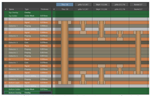
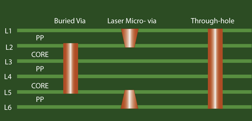
Case study: 8 and 14-layer HDI with Stacked Vias
$ 13.99 · 4.6 (510) · In stock

This case study focuses on the challenges and solutions that we implemented to design complex HDI boards with stacked vias.
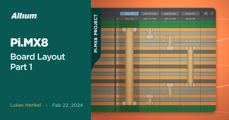
Pi.MX8 Project - Board Layout Part 1

Understanding Proper PCB Design (Part 2) - Circuit Cellar

Multilayer PCB Stackup Planning - Engineering Technical - PCBway

Explain Like I'm a Designer: ELIC PCB and HDI Routing, HDI Design
Advanced High Density PCB Design in Altium Designer
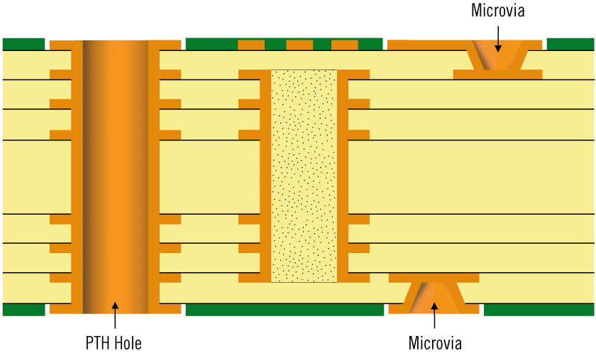
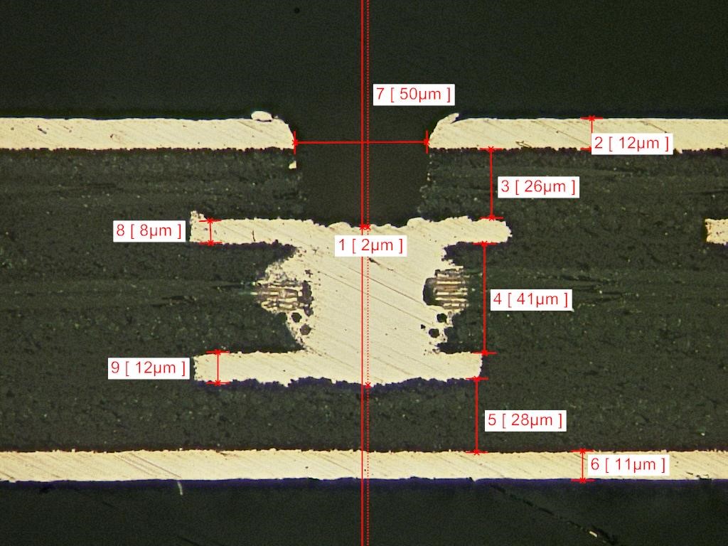
a) SEM-micrograph of the top part of a 10 layer stacked via after

HDI PCB Stackup - Venture Elctronics
Different Stackups for HDI PCBs - Rush PCB
Technologies and processes at ILFA: Sophisticated HDI design in PCB production - ILFA Feinstleiter Technologie
HDI board stack-ups – PCB HERO
The impact of HDI and microvias on PCB design - Tech Design Forum Techniques