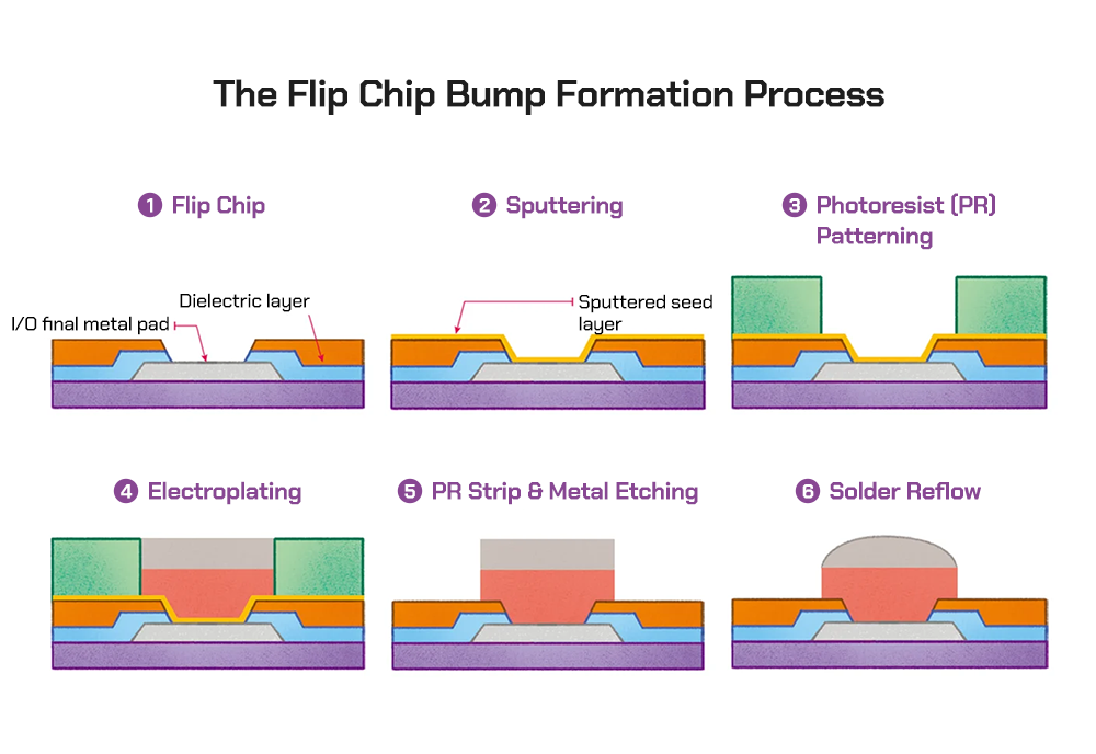
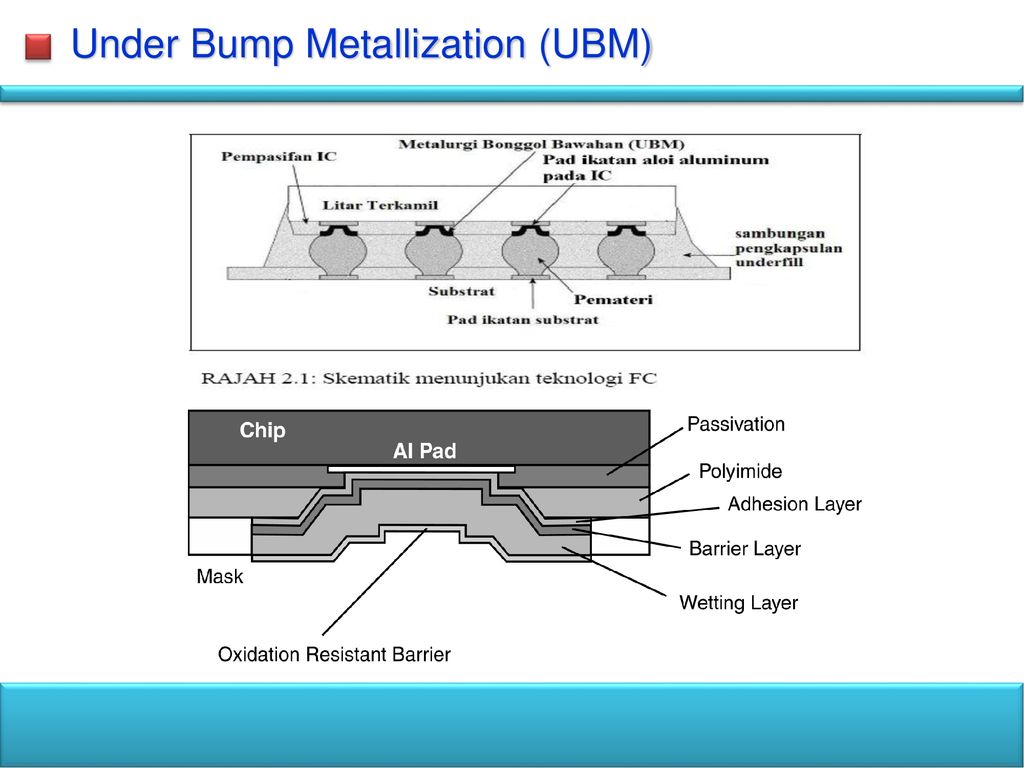
UBM (under bump metallurgy) structure
$ 7.50 · 4.7 (608) · In stock


Figure 8 from Under Bump Metallurgy (UBM)-a technology review for flip chip packaging

Kyung-Wook PAIK Korea Advanced Institute of Science and

Kyung-Wook PAIK Korea Advanced Institute of Science and

PDF) Eutectic Pb/Sn solder bump and Under Bump Metallurgy

Se-Young JANG, Vice Pesient, Ph.D, Samsung, Seoul
d36ae2cxtn9mcr.cloudfront.net/wp-content/uploads/2

Kyung-Wook PAIK Korea Advanced Institute of Science and

Se-Young JANG, Vice Pesient, Ph.D, Samsung, Seoul

PDF) The surface characteristics of under bump metallurgy (UBM) in electroless nickel immersion gold (ENIG) deposition

Figure 6 from Under Bump Metallurgy (UBM)-a technology review for flip chip packaging

Figure 1 from Plasma reflow bumping of Sn-3.5 Ag solder for flux-free flip chip package application
Interconnection in IC Assembly - ppt download