MF181000 - SEMI MF1810 - Test Method for Counting Preferentially Etche
$ 118.50 · 4.7 (73) · In stock

Defects on or in silicon wafers may adversely affect device performance and yield. Crystal defect analysis is a useful technique in troubleshooting device process problems. The type, location, and density of defects counted by this Test Method may be related to the crystal growth process, surface preparation, contamination, or thermal history of the wafer. This Test Method is suitable for acceptance testing when used with referenced standards. This Test Method describes the technique to count the density of surface defects in silicon wafers by microscopic analysis. Application of this Test Method is limited to specimens that have discrete, identifiable artifacts on the surface of the silicon sample. Typical samples have been preferentially etched according to SEMI MF1809 or epitaxially deposited, forming defects in a silicon layer structure. Wafer thickness and diameter for this Test Method is
Defects on or in silicon wafers may adversely affect device
performance and yield.
Crystal defect analysis is a useful technique in
troubleshooting device process problems. The type, location, and density of
defects counted by this Test Method may be related to the crystal growth
process, surface preparation, contamination, or thermal history of the wafer.
This Test Method is suitable for acceptance testing when
used with referenced standards.
This Test Method describes the technique to count the
density of surface defects in silicon wafers by microscopic analysis.
Application of this Test Method is limited to specimens
that have discrete, identifiable artifacts on the surface of the silicon
sample. Typical samples have been preferentially etched according to SEMI
MF1809 or epitaxially deposited, forming defects in a silicon layer structure.
Wafer thickness and diameter for this Test Method is
limited only by the range of microscope stage motions available.
This Test Method is applicable to silicon wafers with
defect density between 0.01 and 10,000 defects per cm2.
Referenced SEMI Standards (purchase separately)
SEMI M59 — Terminology of Silicon Technology
SEMI MF1725 — Practice for Analysis of Crystallographic
Perfection of Silicon Ingots
SEMI MF1726 — Practice for Analysis of Crystallographic
Perfection of Silicon Wafers
SEMI MF1727 — Practice for Detection of Oxidation Induced
Defects in Polished Silicon Wafers
SEMI MF1809 — Guide for Selection and Use of Etching
Solutions to Delineate Structural Defects in Silicon
Revision History
SEMI MF1810-1110 (Reapproved 0222)
SEMI MF1810-1110 (Reapproved 1115)
SEMI MF1810-1110 (technical revision)
SEMI MF1810-0304 (technical revision)
SEMI MF1810-97 (Reapproved 2002) (first SEMI publication)
Guide to Semiconductor Wafer Sort - AnySilicon
LEAD TIME EST. 3-4 BUSINESS DAYS. Calibration standards for 3-inch and 100mm diameter sieves are also available. Contact us for a quote.

Sieve Calibration Standard 75 microns or No.200
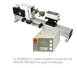
Mark-10 ES30 Manual Force Test Stand
Replacement Stackable Test Lead Pair for Fluke 754 753 75X
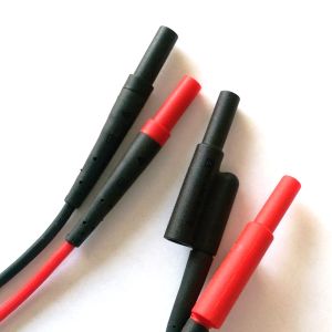
Fluke 75X-8014 Replacement Stackable Test Lead Pair for Fluke, 754 & 753
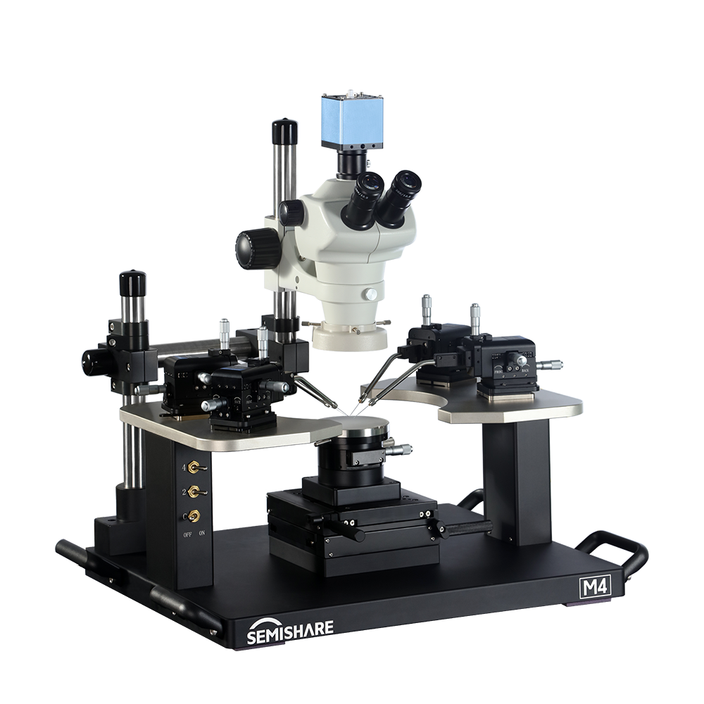
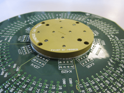
Probe Card for Semiconductor Testing - SEMISHARE Prober

AN-SG2-015: Counter Instructions
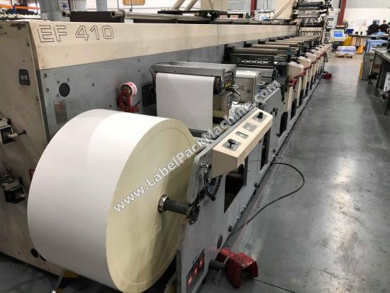
MPS EF 410 second hand, used : Label second hand, used, Flexo second hand, used,LabelPackMachine
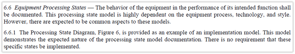
Identifying Custom Test Cases for the SEMI E30 GEM Standard: Part 1
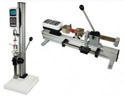
Mark-10 ES30 Manual Force Test Stand
Identifying Custom Test Cases for the SEMI E30 GEM Standard: Part 1

Sand equivalent test set
FedPro CR1000 Contact Image Sensor Value Counter – Carnation Bill Money Counting Machines

EC-100 Counter with SPC Output from Mitutoyo