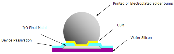
Bump on Pad, Wafer Process Technology
$ 4.99 · 4.8 (98) · In stock
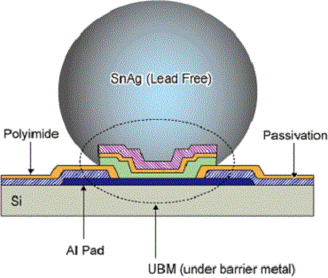
Bump on Pad Key features include: Wafer process and bumping in consolidated assembly. Technology supporting wide range of products from mobile devices to
Wafer with pad, bumps and daisy chain partial layout (quarter of die
Prestige Popular Stainless Steel Pressure Cooker, Litres

Figure 11 from Copper pillar bump technology progress overview

Heterogeneous Integration and IC Packaging - EE Times Europe
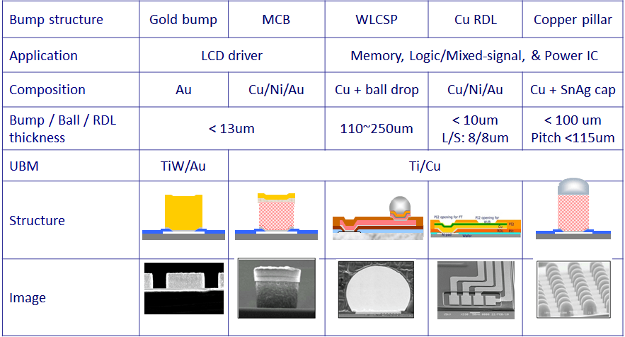
ChipMOS TECHNOLOGIES INC. – Back-end testing service for memory, LCD Diver, Bumping and MEMS.
)
Prestige Popular Stainless Steel Pressure Cooker, Litres
d36ae2cxtn9mcr.cloudfront.net/wp-content/uploads/2
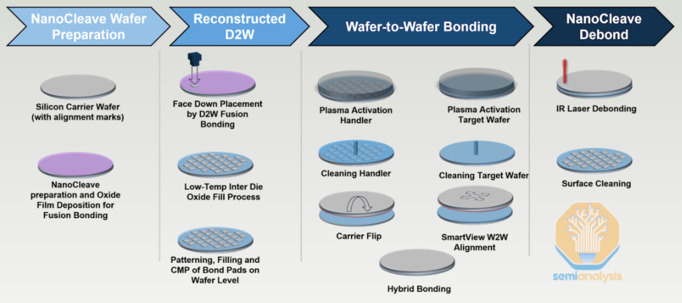
Hybrid Bonding Process Flow - Advanced Packaging Part 5
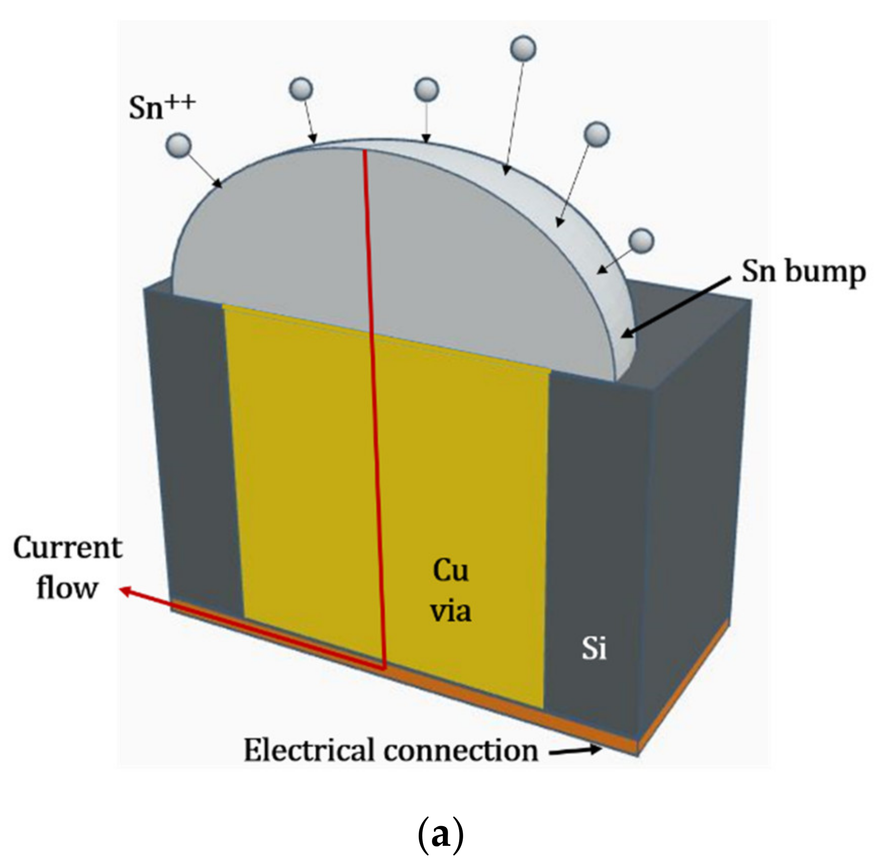
Metals, Free Full-Text
FlipChip

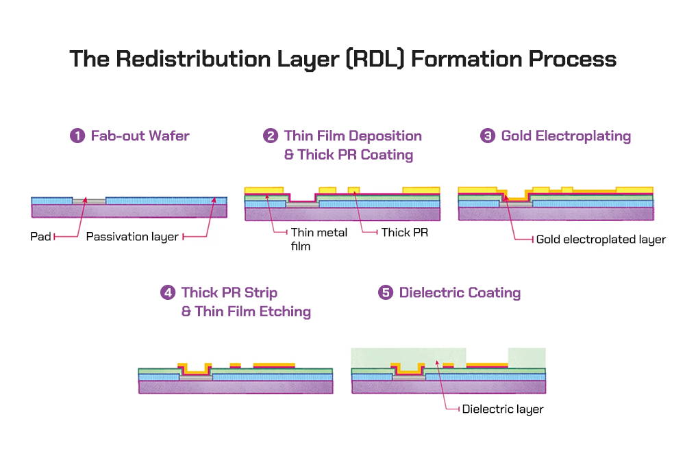
Wafer Cross-Sections Through the Bumping Process

Fine‐Pitch Solder on Pad Process for Microbump Interconnection - Bae - 2013 - ETRI Journal - Wiley Online Library